layout design rules ppt
Diffusion and Tap Width and Space Martin p44 Cypress nwell Diff-tap poly Pdiff Minimum width. Static CMOS Series and.
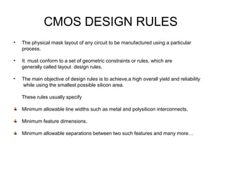
Layout Design Rules 2 Introduction Layout Rules Is Also Referred As Design Rules It Is Considered As A Prescription For Preparing Photomasks Ppt Download
See more ideas about powerpoint presentation design powerpoint design templates powerpoint design.
. Next lets look at some of the key design rules for PCB layout starting with how the rules should begin in the schematic. Design rules are consisting of the minimum width and minimum spacing requirements between objects on the different layers. The most important parameter used in design rules is the minimum line width.
Wire widths to avoid breaks min. Jan 12 2020 - Explore Warangs board ppt guideline on Pinterest. Minimum line width scalable design rules.
Layout design rules. Sketch a 4-input CMOS NAND gate CMOS Gate Design Activity. Simple for the designer.
The courses are so well structured that attendees can select parts of any lecture that are specifically useful for them. 2 Freescale Semiconductor 3 Another factor to affect signal performance and noise separation is transmission line effect and modeling. Trace timing or tuning.
Sketch a 4-input CMOS NOR gate Complementary CMOS Complementary CMOS logic gates nMOS pull-down network pMOS pull-up network aka. 5 Step Sticker Banners for PowerPoint. Layout and Rules Reasons behind Rules.
Differential pair trace routing. Provide feature size independent way of setting out mask. The USP of the NPTEL courses is its flexibility.
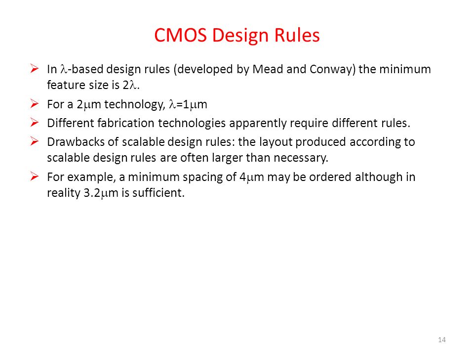
Layout continuity from frame to frame conveys a sense of completeness Headings subheadings and logos should show up in. Register for exams Timelines and Guidelines Course Booklet Part 1 Part 2 Part 3 Part 4. Lambda Based Design Rules.
CMOS Layout Layout design rules describe how small features can be and how closely they can be reliably packed in a particular manufacturing process. Minimum distance rules between device layers eg polysilicon metal metal metal diffusion diffusion and minimum layer overlaps are used during layout Layout design rule checker DRC automatically verifies that no design rules have been broken Note however the use of Lambda is not optimal but supports design reuse. Layout design rules are introduced in order to create reliable and functional circuits on a small area.
Main terms in design rules are feature size width separation and overlap. Outline CMOS Gate Design Pass Transistors CMOS Latches Flip-Flops Standard Cell Layouts Stick Diagrams CMOS Gate Design Activity. Design Rules Jan M.
Our PowerPoint layout design templates can be used to make good presentations in a matter of minutes from project timelines list slides and even diagrams depicting a process. Layer rules unique spacing and specific widths for controlled impedance routing. For working professionals the lectures are a boon.
Design rules does represent geometric limitations for for an engineer. Transmission line is a trace and has a distributed mixture of resistance R inductance L and capacitance C. Width of pMOS should be twice the width of nMOS.
Design rules based on single parameter λ. Rabaey Cross-Section of CMOS Technology Design Rules Interface between designer and process engineer Guidelines for constructing process masks Unit dimension. Spacing to avoid shorts minimum overlaps to ensure complete overlaps Measured in microns Required for resolutiontolerances of masks Fabrication processes defined by minimum channel width Also minimum width of poly traces Defines.
This post covers introduction to layout design rules. 1 Peak doping concentration needs to be repeatable independent of width or the lateral diffusion 2 Photoresist must have a minimum opening to allow the implant. Power net rules for wider widths and clearances.
A layout is just a set of rectangles where each rectangle. This video on Know-How series helps you to understand the different set of layout design rules. DESIGN RULES Design rules define ranges for features Examples.
PowerPoint Presentation Guidelines Highlight key points or reinforce what the facilitator. 3 Must be wide enough to enclose a contact. The layout design rules provide a set of guidelines for constructing the various masks needed in the fabrication of integrated circuits.
Design Rules EE213 VLSI Design Stick Diagrams VLSI design aims to translate circuit concepts onto silicon stick diagrams are a means of capturing topography and layer information - simple diagrams Stick diagrams convey layer information through colour codes or monochrome encoding Used by CAD packages including Microwind Design Rules Allow translation of. Lambda parameter absolute dimensions micron rules CMOS Process Layers Intra-Layer Design Rules Transistor Layout Vias and Contacts Select. Create custom PowerPoint Diagrams Project Timelines and Thank You slides with these gool PowerPoint Slide layouts for.
Lambda-based rules are necessarily conservative because they round up dimensions to an integer multiple of lambda. Layout Design rules Lambda Same N and P alters symmetry L min Wpmos2 Wnmos. Fonts Font Style Should be Readable Recommended fonts.
Design Consideration High Speed Layout Design Guidelines Application Note Rev.